
The bottom line
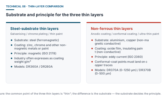
“Thin layer” is not the basis for selection — the substrate is. At tens of microns, galvanising uses magnetic and anodic coating uses eddy current; the difference comes from the substrate side.
The three side by side
| Dimension | Galvanising | Anodic coating | Conformal coating |
|---|---|---|---|
| Substrate | Steel (ferromagnetic) | Aluminium (non-magnetic conductive) | Copper foil (non-magnetic conductive) |
| Coating nature | Non-magnetic metal (zinc) | Insulating oxide layer | Insulating polymer |
| Measurement principle | Magnetic (ISO 2178) | Eddy current (ISO 2360) | Eddy current (ISO 2360) |
| Related standard | ASTM B499 / E376 | ISO 2360 / GB/T 4957 | ISO 2360 |
| Expression habit | Coating weight g/m² or μm | μm | μm or mil |
| Special limit | Rough surface, thicker at edges | Recalibrate when alloy grade changes | Point must be on copper foil |
1. Galvanising: watch the conversion and roughness
Measuring galvanising thickness itself is not hard; the difficulty is in two points:
- Unit conversion: the industry habit is to express as coating weight, so thickness must be converted to g/m² using zinc density. The conversion factor should follow the project spec or supply agreement;
- Surface non-uniformity: hot-dip galvanised surfaces have spangle and zinc nodules, and edges run thick; more points are needed and edge data must be recorded separately.
2. Anodic coating: the “cleanest” measurement target
The oxide film is insulating, grown in place, with a flat interface — the ideal eddy-current target. Only one thing needs attention: changing the aluminium alloy grade requires recalibration, because different grades have different conductivity and the reading baseline shifts accordingly.
3. Conformal coating: point location decides success
Conformal-coating measurement has a limit the other two do not: eddy current needs a conductive substrate to form a circuit, yet much of a circuit board is non-conductive fibreglass substrate. Therefore the measurement point must land above the copper traces.
This adds a pre-step to the workflow: first confirm the copper-trace position with a magnifier or AOI image, then aim the probe at the trace. In practice the point location is fixed in the work instruction to keep data comparable between batches.
Range and model selection
| Thin-layer type | Typical range need | Dongru model |
|---|---|---|
| Galvanising (general) | 0-1250 μm is enough | DR360A (0-2000 μm, with coating-weight conversion) |
| Anodic coating (decorative) | 0-500 μm to 0-1250 μm | DR370B / DR370A |
| Anodic coating (hard, thicker) | 0-1250 μm or above | DR370A / DR380A |
| Conformal coating | 0-500 μm or 0-1250 μm | DR370A / DR370B |
| Ultra-thin oxide layer | 0-500 μm | DR370B |
Common misconceptions
- “All thin layers need the same instrument” — different substrates mean different principles, so the instrument is not interchangeable.
- “Any spot on a conformal board can be measured” — only above the copper foil is valid.
- “Thicker galvanising protects better” — too thick adds brittleness and hurts fit; specs usually set an upper limit.